

As you know, the problem is easier to prevent than to deal with its consequences. Sometimes the consequences are irreversible. In relation to the production of electronics that truth can be applied to a manufacturing defect. Easier and more cost-effective to identify and potentially caused any defects in the early stages of production and to eliminate them than receiving endless complaint and expend considerable resources to repair and maintenance.
| Testing in prototyping | |
Input control | Testing in the manufacture |
|||||||||
|
|
 |
|
|
|
|
|
|
|||||
| Automated Optical Inspection |
The in-circuit inspection |
Peripherals scan | Functional testing |
Test the final product | ||||||||
| |
|
The |
||||||||||
 |
|
 |
|
 |
|
 |
|
 |
|
|
|
 |
| product Development |
Purchase of components | marking | Storage components | manufacturing | Storage of finished products | Implementation | ||||||
| The process of electronics manufacturing and testing stages | ||||||||||||
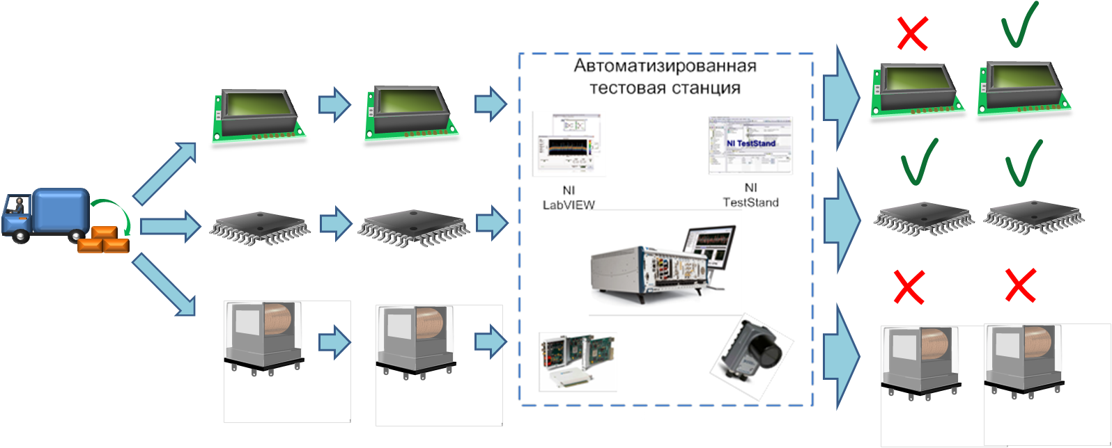
Electronics is a multi-step process. The more frequent and rigorous detection of defects occurs, the higher the probability of high product yield with desired properties and the desired service life. At different stages of the production of a variety of control methods used to perform specific tests. The following shows the basic methods and techniques of production control, we offer the design and delivery of turnkey for your production:
Automated input control
Automated control input (Receiving Inspection) main components (integrated circuits, microprocessors, LCD displays, power devices, and cable assemblies) contributes to a significant increase in product quality. The process as a sort of accessories to fit / unfit for production and their classification by variation of electrical and technical specifications. On the storage and production workers get guaranteed products and products sorted for endpoints.
 |
| Automated control input for rejection and sorting components |
We offer to develop a system for input control on the PXI platform. These are high-speed multifunctional systems that will allow you to produce both sequential (in turn) and parallel (all devices simultaneously) testing of products supplied to your enterprise. The system includes a PXI measurement system, NI LabVIEW test application development environment, and NI TestStand automated test management environment. As a supplement, we use automated optical inspection (AIO) to determine mechanical and geometric defects, determine the volumes and areas of products, which we create based on the NI Vision Builder environment and technical tools for working with real-time images (video capture boards, PXI systems) , video cameras, lights, conveyor, etc.)
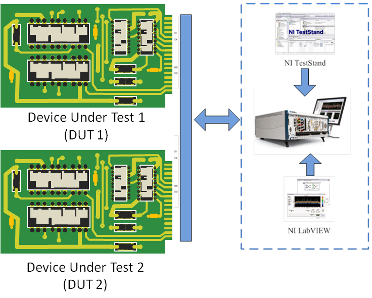
Automated in-circuit inspection (In-Circuit Test)
In-Circuit Test (ICT) is a very powerful tool for testing assembled and sealed PCBs. By creating a connection between the test system and the printed circuit board using a bed of nails, flying probes or a cable assembly, it is possible to check the functioning of each individual component (or group of components) independently of the electrically connected components. Thus, short circuits, ruptures, no soldering or component, resistance, capacitance, and other basic electrical characteristics are verified, by which one can judge the correctness of the assembly of the printed circuit board.
The figure shows a diagram of a system in-circuit testing. Here, the printed circuit board is installed in the fixture. Fixture has a probe sets that hit the test pads on the printed circuit board when you close the lid of the test fixture. The test fixture is connected with the cable ssitemoy test, which is based on the NI PXI platform. Configured test suites are run automatically in the NI TestStand environment.
.png) |
| The station for in-circuit testing |
We are developing a system for in-circuit testing under the special needs of the customer. The system comes with I / O modules, which cover the needs of any production, including high-frequency equipment.
Boundary Scan (Boundary Scan)
Boundary Scan Method (Boundary Scan) also known as JTAG or IEEE 1149 is a very important tool for testing printed circuit boards and electronic devices during development, production and operation. boundary-scan method allows you to test the device with minimal connections. As JTAG, boundary scan method does not require the presence of test probes, "bed of nails" or other methods of contact with the circuit board. This method provides a unique opportunity for many test applications and tasks:
- testing at the system level;
- emulation CPU, MCU;
- Programming FPFA / CPLD on the board;
- memory test;
- programming of FLASH-memory on the board;
- access to the subsystem self-test of the integrated circuit;
- testing the quality of soldering (particularly BGA components);
- effective and rapid diagnosis of the defective unit or the entire device.
 |
| Parallel connection of two test printed circuit boards to the boundary-scan system (Boundary Scan Test System) |
For the production problems of the enterprise, we will design and develop the system in a short time boundary-scan. The system will allow testing, programming and diagnostics fast and efficient, freeing up time for other important production tasks. Tools for creating test systems are traditionally Boundary Scan controllers, I / O modules and the PXI format and PXIe, NI LabVIEW programming environment and NI TestStand test management environment.